About the Class
In both the local and global class we were introduced into the theoretical concept and process of PCB milling and soldering. This extended into a hands-on introduction of soldering top-mounted components on PCB boards and handling the Roland SRM-20 mill. More on the details below.
Learning how to solder
After a theoretical introduction, we were given the chance to practice soldering hands-on. For that, we had special text boards with varying practical difficulty throughout board. After the intro, I had the chance to solder a lot more as it turned out: By building a 4-track collaborative loop station in the Fab Academy challenge week, we needed some 30+ connections to be soldered. After a couple of hours, I became more confident and quicker with soldering.
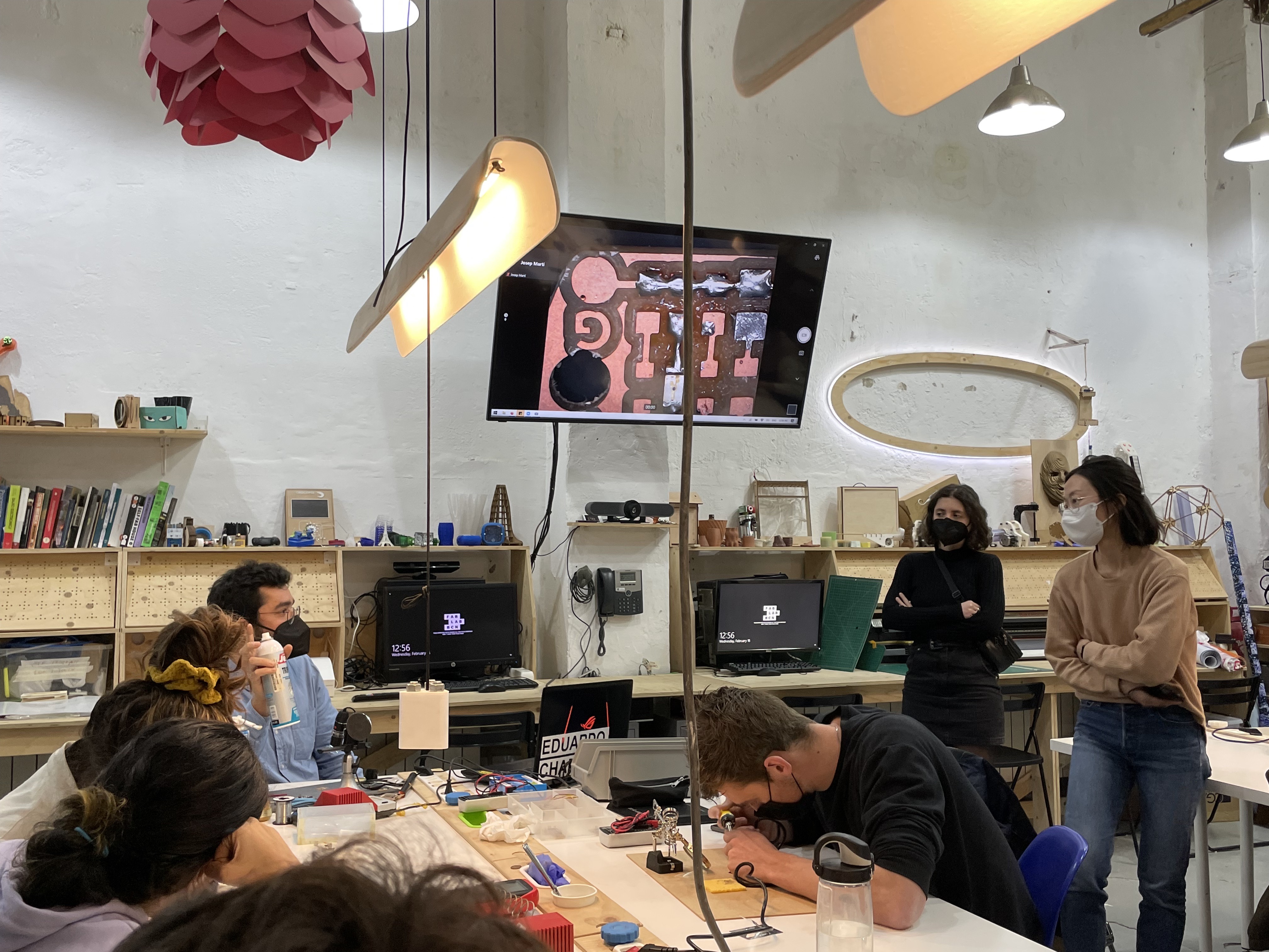
Eduardo explaining the ways to correctly place and solder components on a milled PCB board.
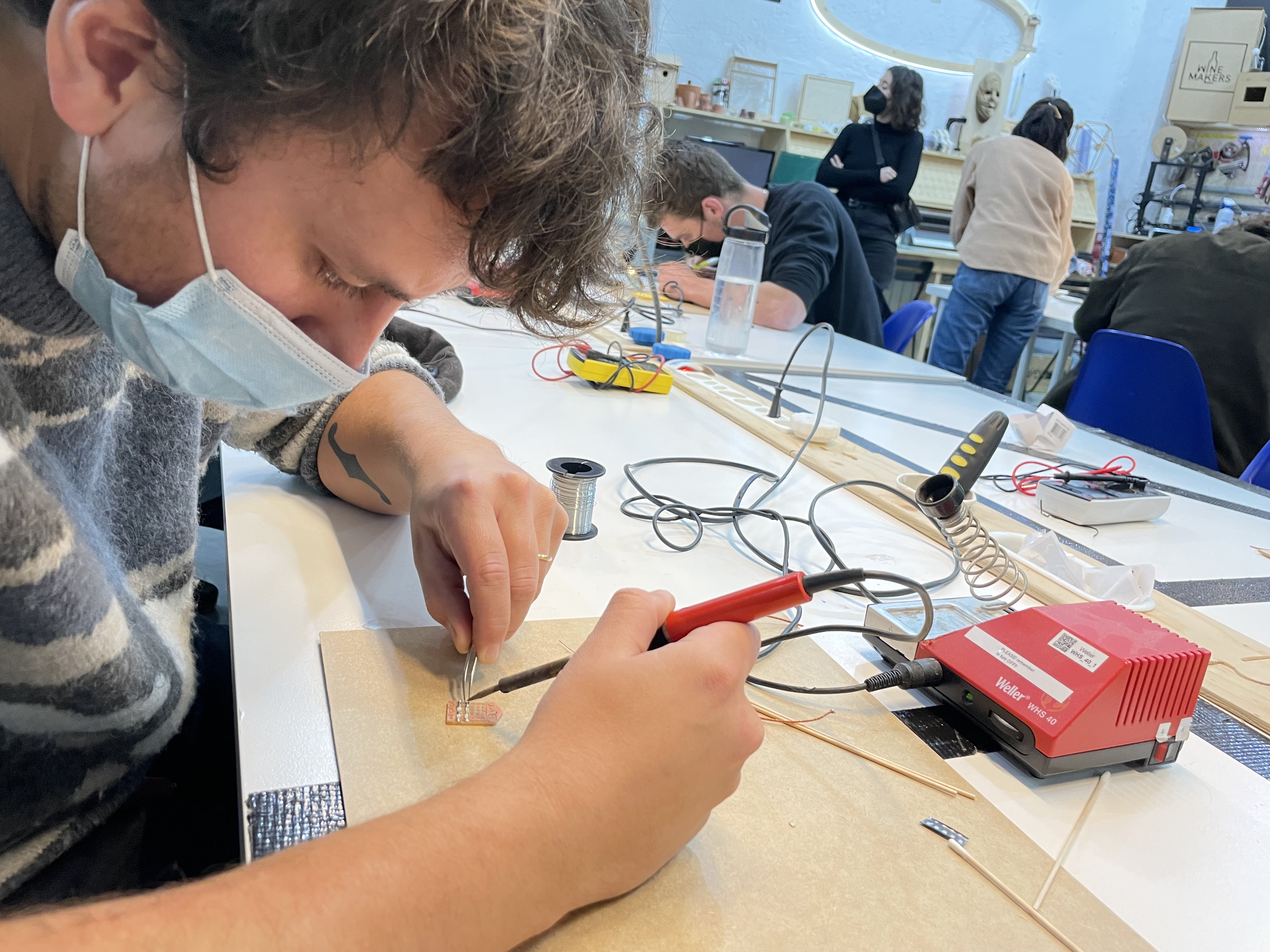
Joaquin practicing on the soldering test board.
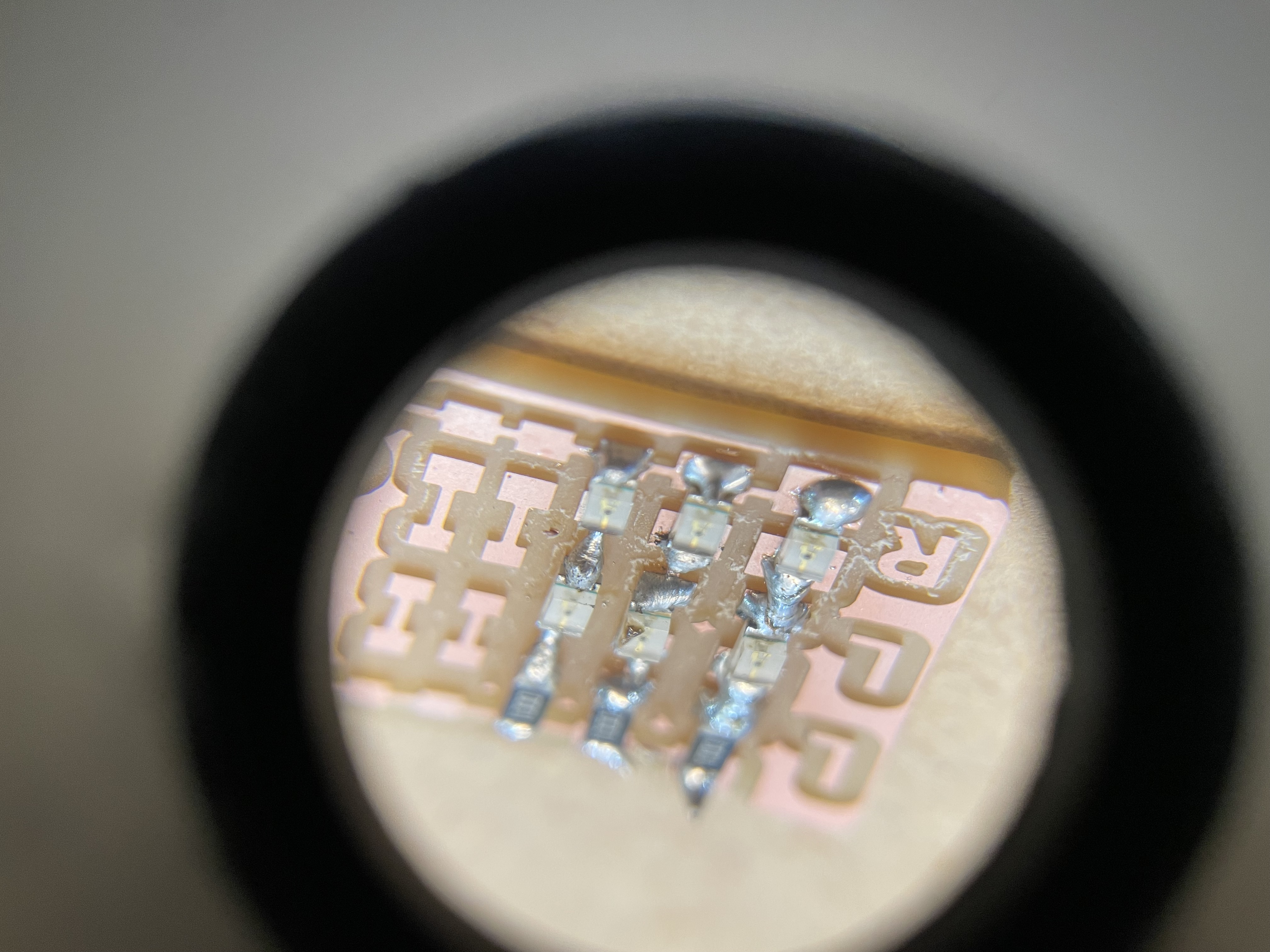
The result of practicing on the test board under a magnifying glass. From left to right, the quality of the solder connections can be seen (although still not incredibly great).
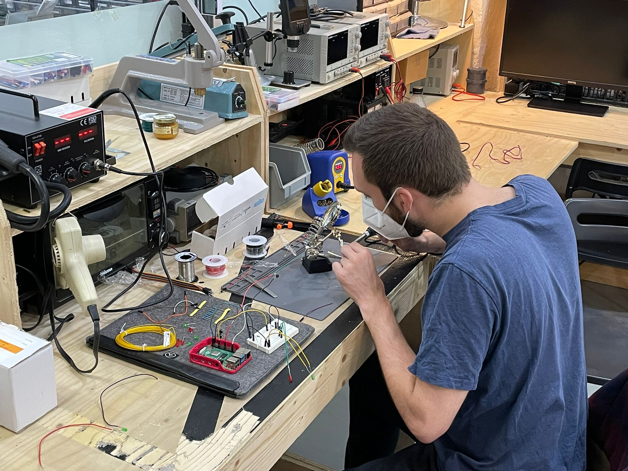
Honing my soldering skills during the first Fab Academy Challenge, soldering some 30+ connections.
PCB Design and Milling
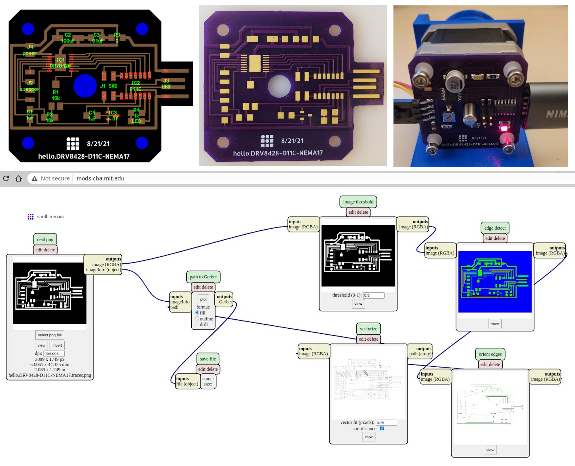
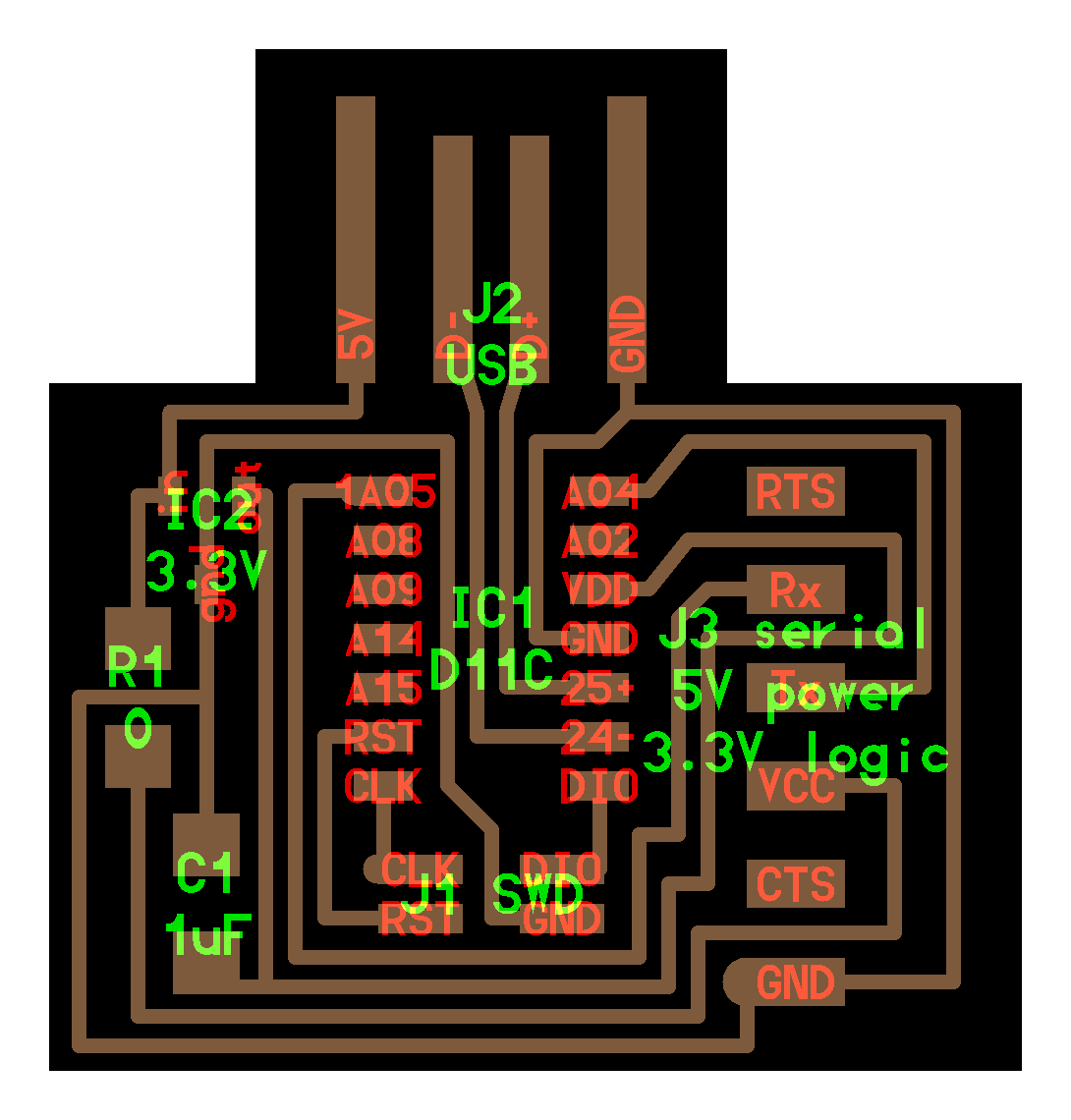
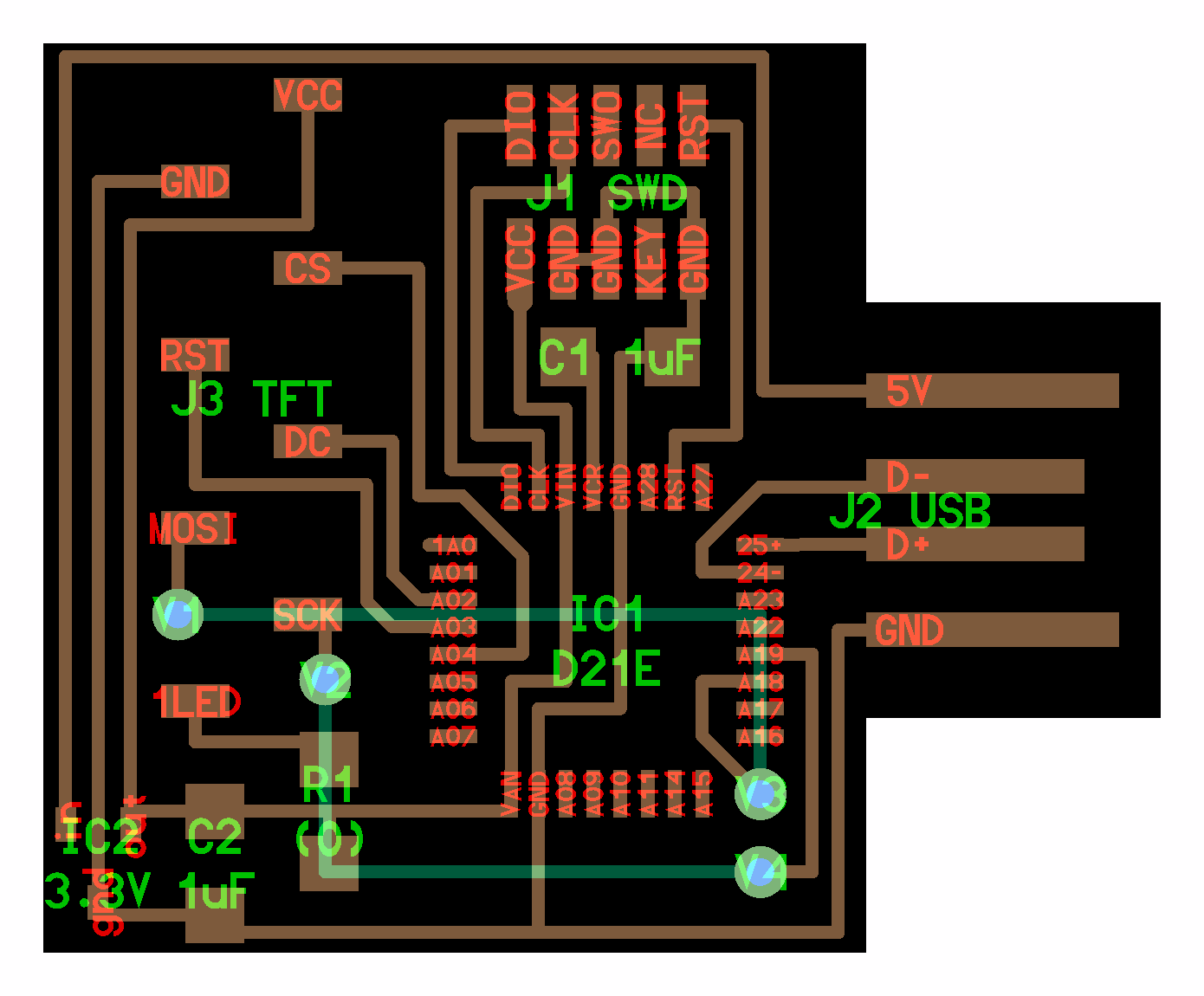
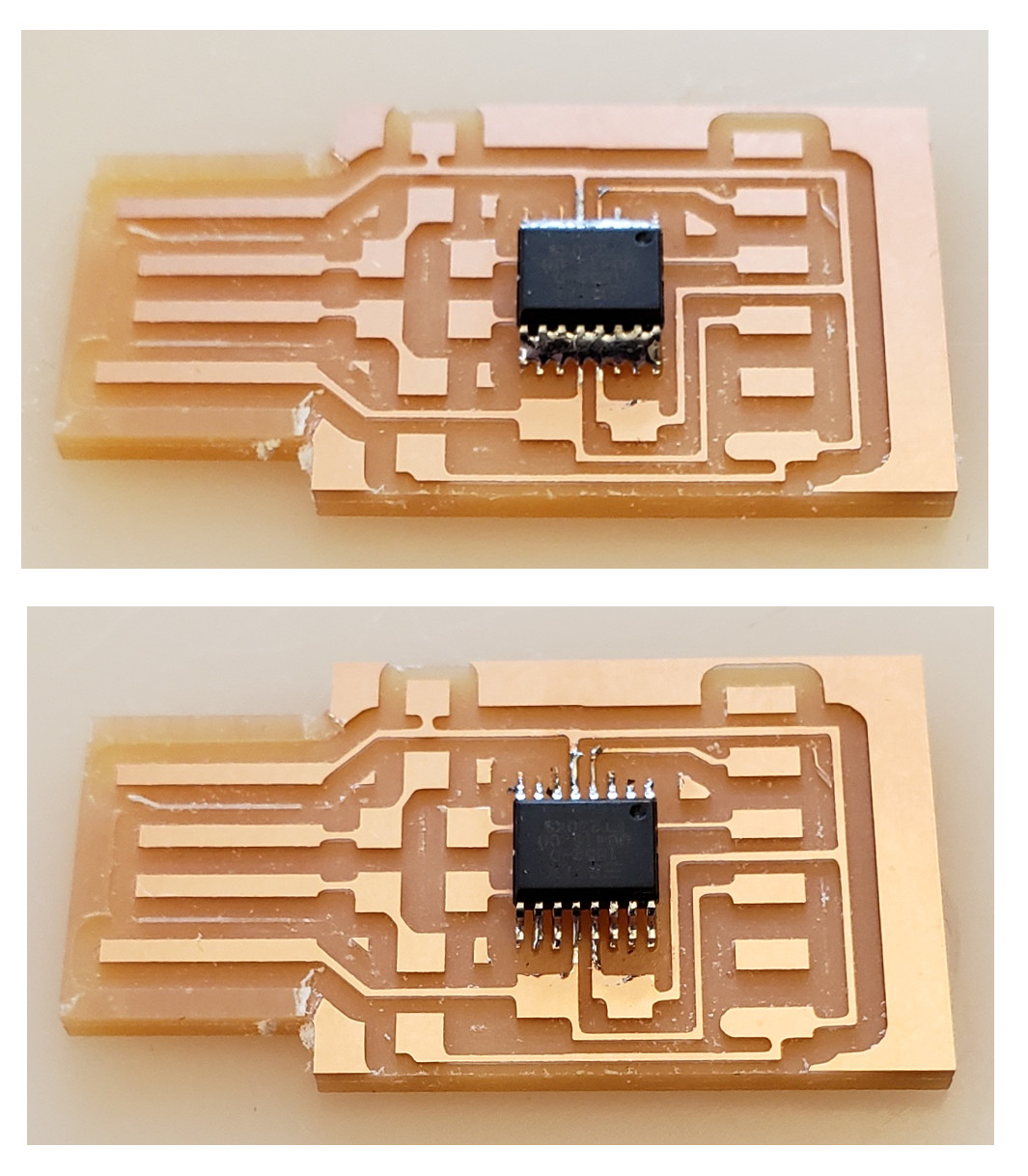
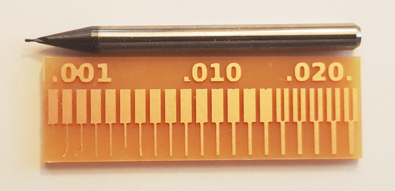
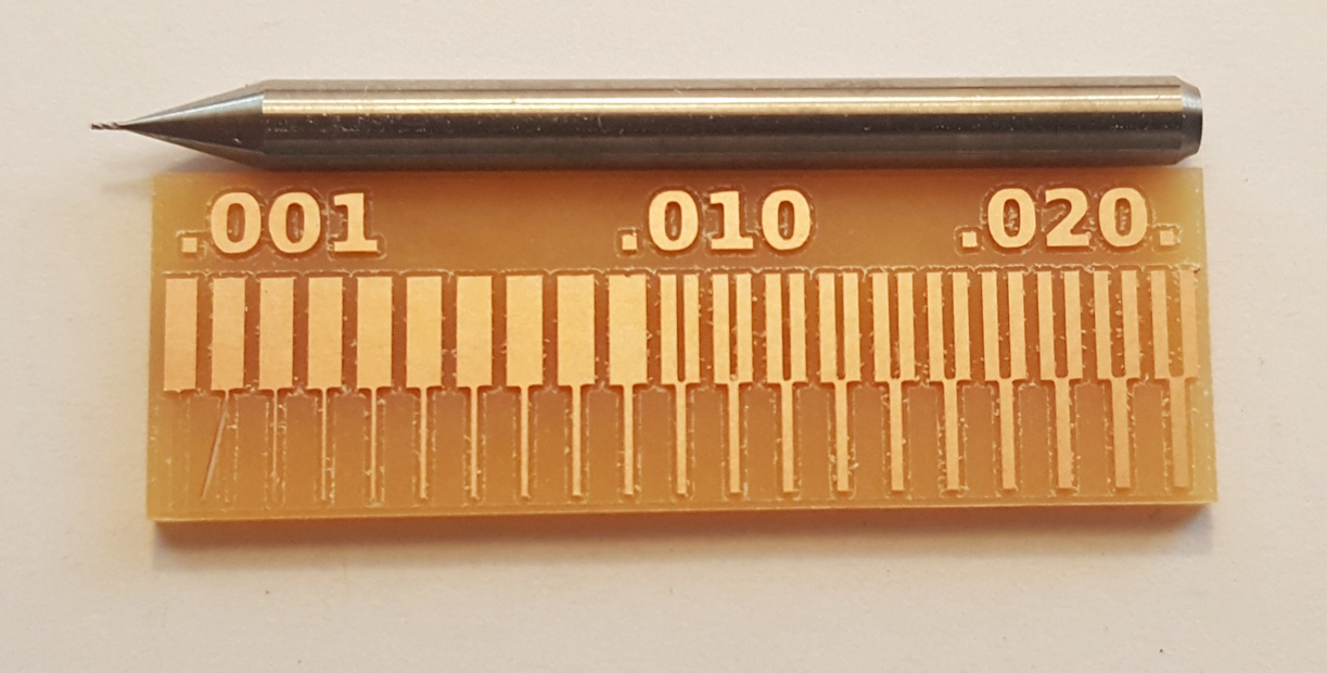
As for the custom PCB design and milling, one of the most important concepts is to understand how the drill moves across and through the copper layer on the substrate plate. To prepare high-resolution PNGs or SVGs for milling, we generate Gerber-files via Modsproject, which is a node-based formatting online tool developed and open-sourced by the MIT. In order to generate the files for the specific mills at the FabLab BCN, we need to open a new program (right click on canvas) and select Roland SRM-20 mill > PCB Absolute as settings.
After soldering for a while during the first Fab Academy challenge week, the next step for the loop station should be to design a custom PCB board to reduce the amount of cables and the need for a breadboard. This will allow for a better layout of the components and a smaller physical footprint, since it can be implemented as a shield for the Raspberry Pi 4. I'm currently diving into Fritzing to learn how to design such a board exactly.
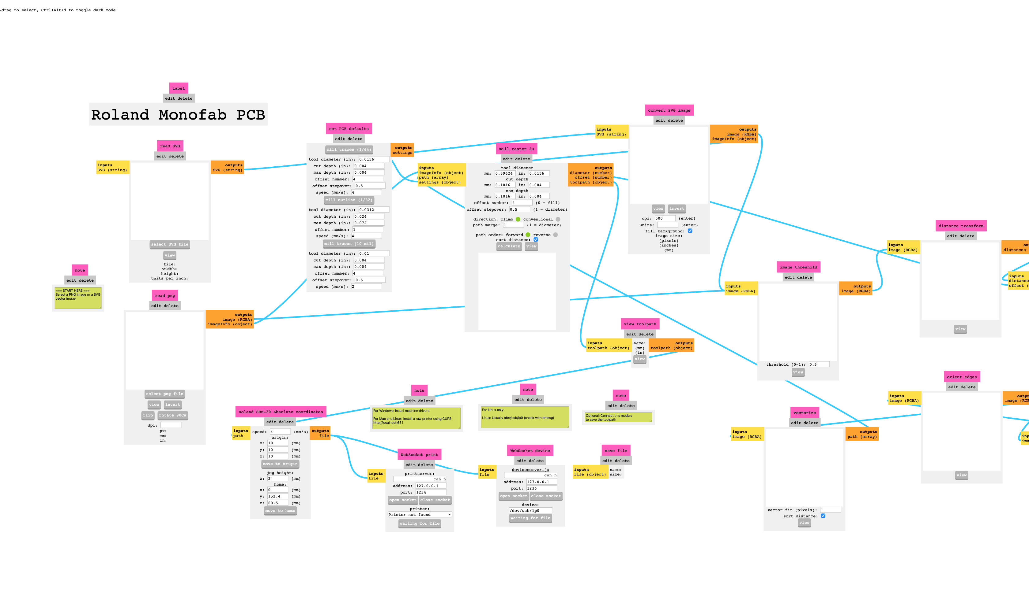
The modsproject nodes for processing a PCB design for the Roland SRM-20 mill.
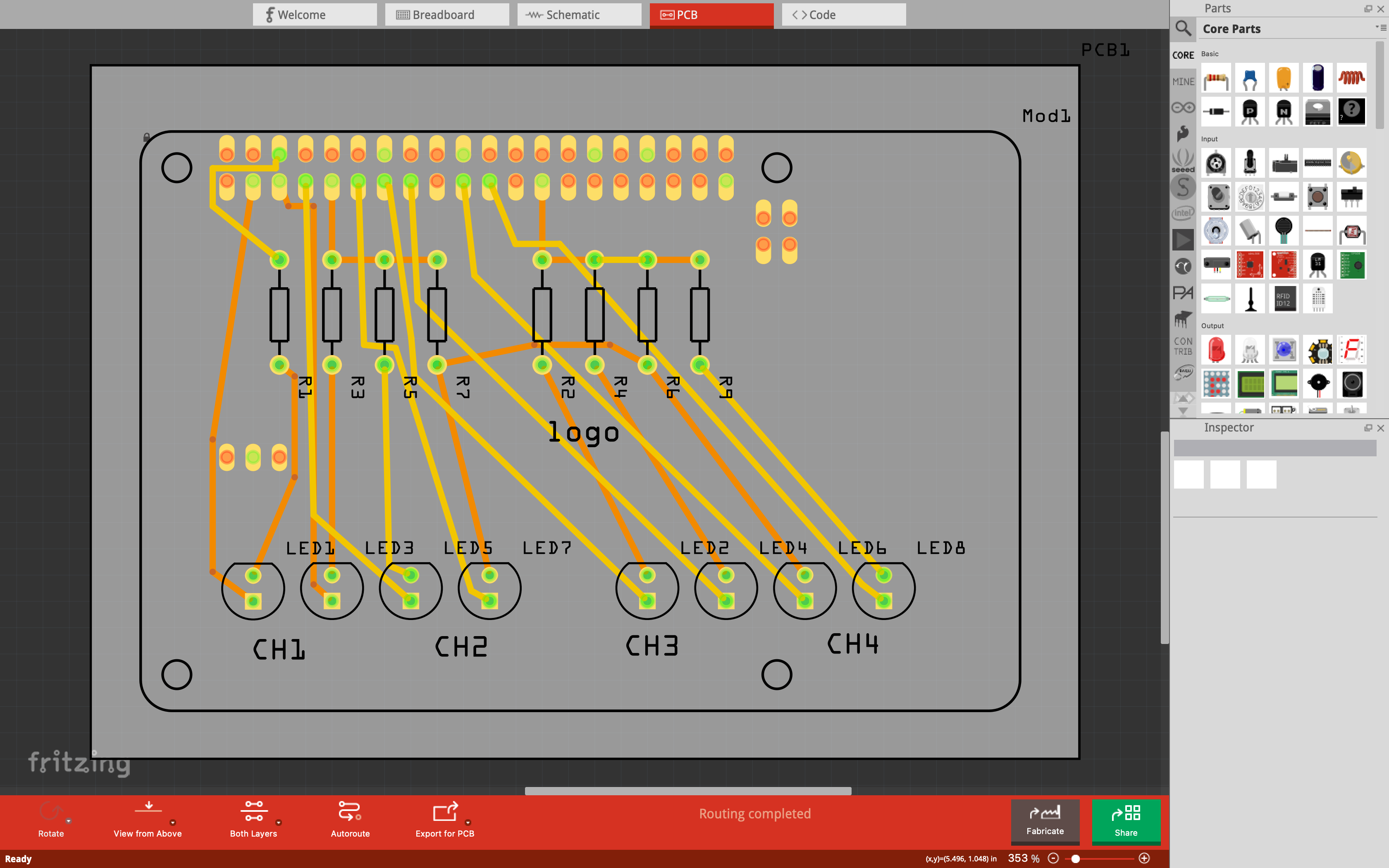
Getting started designing a custom Raspberry Pi shield in Fritzing.
Further Links
PCB fabrication
etching
lithography, transfer
ferric/cupric chloride, ammonium/sodium persulfate
citric acid, peroxide
SDS
water consumption
waste
machining
machines
tools
0.010
1/64
1/32
V-bits
tapered bits
contouring bits
fixturing
underlay
orientation
zeroing
set-screws
lifetime
deburring
cleaning
climb vs conventional
vinyl cutter
flex
connections
encapsulation
milling
laser cutter
printing
conducting inks
plating
sewing
PCB materials
rigid
FR4 (epoxy glass)
FR1 (phenolic paper)
garolite
flex
Kapton, Pyralux
#1 epoxy film, #1126 copper tape
high-frequency
teflon
glass
copper
0.5 oz: 17.5 um
1.0 oz: 35 um
2.0 oz: 70 um
board houses
OSH Park, JLCPCB,
DKRed, Advanced, PCB:NG, Sierra, Screaming Circuits,
PCBWay
,
AQS, Gold Phoenix, 3PCB, Seeed,
Think & Tinker
PCB, kit, BOM
design rules
width/spacing (15, 5 mils)
layers
1, 1.5, 2, 2+, 4, N
mechanical, drill, solder mask, silk screen
vias
rivets, plated, blind, buried
components
through-hole
surface-mount
chip-scale
breadboards
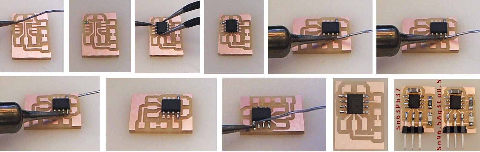
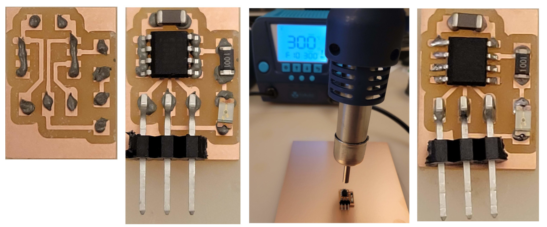
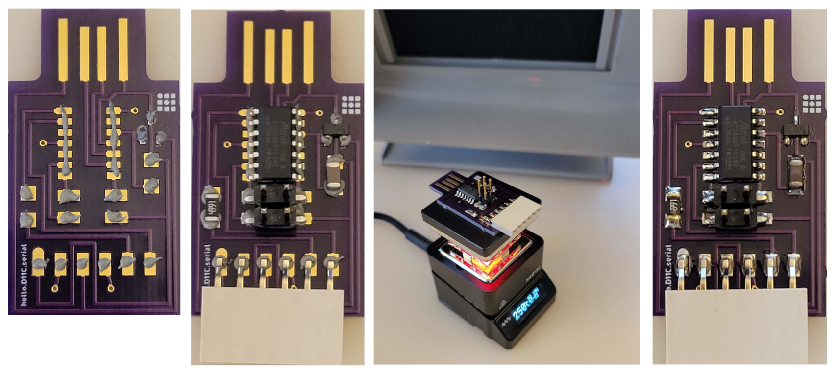
assembly
solder
iron
station
fume extractor
ROHS
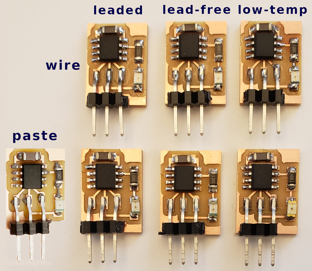
types
lead-free wire
paste
SDS
leaded wire
paste
SDS
low-temp wire
paste
eutectic
wetting
manual, drag, wave
cold solder joints
flux core, paste, pen
reflow
hot air, hot plate, oven, IR
magnifying
stuffing
component orientation
tacking down parts
bottom to top, inside to outside
fumes
washing
desoldering
braid
vacuum
hot air
gravity
cutting traces, adding jumpers
pick-and-place
encapsulation
CAM
formats
Gerber/RS-274X
png resolution
FlatCAM
cam.py → cad.py → kokompe → fab modules → mods
community edition
video
trace width
traces
interior
1/64"
0.010"
fiber laser
assignment
group assignment:
characterize the design rules for your in-house PCB production process
extra credit: send a PCB out to a board house
individual assignment:
make an in-circuit programmer that includes a microcontroller:
extra credit: customize the design
mill and stuff the PCB
test it to verify that it works
extra credit: try other PCB processesamet, consectetur adipiscing elit. Suspendisse varius enim in eros elementum tristique. Duis cursus, mi quis viverra ornare, eros dolor interdum nulla, ut commodo diam libero vitae erat. Aenean faucibus nibh et justo cursus id rutrum lorem imperdiet. Nunc ut sem vitae risus tristique posuere.